
| Cerius2 Builders |
This chapter contains information on:
The sequence of steps for using the C2·Interface Builder module is shown below. These steps are described in more detail later in the chapter.
1. Define the right side of the interface--Specify the crystal
model, Miller plane, match vector, match point, and dimensions
of the right side of the interface.
Controls belonging to the C2·Interface Builder module are contained on the INTERFACE BUILDER card, which is located by default on the BUILDERS 1 deck of cards. To access the INTERFACE BUILDER card, click its name to bring it to the front of the deck of cards, which should now look like this:
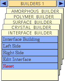
To construct an interface, you need to define the two sides of the interface, specify some build-control parameters, and then build the interface. Afterwards you may need to remove superimposed atoms from the interface.![]()
Creating an interface
The starting model(s)
For each side, you need to specify a crystal model from which to take the interface. The model is chosen from the Interface Model pulldown (the left and right control panels contain the same set of controls), which show only crystal models that are suitable for use with the interface builder. The model needs to be chosen first.
The interface Plane itself is specified by the Miller indices h, k, and l. The convention is that the vector coming out of the built interface (that is, towards the other side) is normal to the interface plane. For the right side of the interface, the vector normal to the Miller plane points in the negative x direction. For the left side of the interface, this vector points in the positive x direction.
The Match Point specifies a point in crystal fractional coordinates that should match the match point of the other crystal. The match point is also the origin of the interface slab to be cut from the crystal. If the interface separation is zero, the match points coincide. If not, their projections normal to the interface planes coincide.
For each crystal, a match vector must be defined as the First Side of Interface Mesh. Because the two interface planes must be oriented with their match vectors parallel, the match vector and match point together define the relative orientations of the two planes. The match vector is given in the u, v, w fractional coordinate system of the crystal, and the interface builder checks that the vector is indeed in the interface plane. When the interface is built, this vector lies along the z axis.
Constructing the starting model
Load or build one or two crystals from which the interface is to be constructed.
Open the Interface Right Side control panel by selecting the Right Side menu item from the INTERFACE BUILDER card. Alternatively, if you have the Interface Building control panel (see Accessing the tools) open, click its Right Side... pushbutton.
Open the Interface Left Side control panel by selecting the Left Side menu item from the INTERFACE BUILDER card. Alternatively, if you have the Interface Building control panel (Accessing the tools) open, click its Left Side... pushbutton.
From the Interface Model pulldown, select the crystal to be used to generate a side of the interface.
Enter the Miller indices of the interface Plane.
| To use the location of a particular atom as the match point, <Shift>-click the atom with the right mouse button. The atom's coordinates appear in an information box. |
Please see the on-screen help for additional information about the controls in all the panels mentioned here.
Building the interface
Once the interface has been correctly defined on both sides, you are ready to build the interface. This is done with the Interface Building control panel.
The interface is built from the two sides specified in the Interface Left Side and Interface Right Side control panels. The build operation takes place in the current workspace, which must be empty. The original crystals are not affected by the interface building.
After defining the interface sides as described above (Specifying the sides of the interface), open the Interface Building control panel by selecting the Interface Building menu item on the INTERFACE BUILDER card.
Set the dangling bonds popup according to how you would like dangling bonds to be displayed. They may be omitted altogether (NEITHER), drawn on the LEFT or RIGHT side only, or drawn on BOTH sides of the interface. Dangling bonds are a representation of bonds that existed in the crystal across the cleave face of the interface. The atom that is not in the cleaved set is replaced by a dummy atom. Use of this option gives an indication of the bonding patterns that may be required across the interface.
When the Remove superimposed atoms box is checked, atom pairs at the interface that are superimposed (within the Superimposition tolerance) are replaced by one atom from the interface side specified by the Keep atoms popup. Any bonds to the removed atom are transferred to the retained atom.
After the build parameters have been specified, make an existing empty model space current or open a new empty model space.
Building the interface
Click the BUILD INTERFACE pushbutton. The new interface is built in the current (empty) model space.
Please see the on-screen help for additional information about the controls in all the panels mentioned here.
Editing the interface after it is build
After the interface is built, the Edit Interface control panel gives you a second chance at removing superimposed atoms, without requiring you to rebuild the interface. This option removes all duplicate atoms and transfers the bonding to the retained atoms.
Open the Edit Interface control panel by selecting the Edit Interface menu item from the INTERFACE BUILDER card.
With the interface in the current model window, click the REMOVE DUPLICATES pushbutton. The Superimposition tolerance entry box on the Interface Building control panel also controls the tolerance for duplication here.
Please see the on-screen help for additional information about the controls in all the panels mentioned here.
This section includes information on:![]()
Creating a periodic model from an interface
When an interface is built, it is oriented in a way that makes creating a periodic model from the interface model straightforward.
In addition, the crystal and surface cell parameters are set so that building a crystal or surface from an interface model puts the interface in a reasonable plane and assigns default cell or mesh parameters that match the dimensions of the right side of the interface. This enables you to extend interfaces, particularly those where the two sides match. For example, this is necessary for performing HRTEM simulations on an interface, because HRTEM calculations can be applied only to crystal models.
Accessing the tools
Open the Crystal Building control panel by selecting the Crystal Building menu item from the CRYSTAL BUILDER card.
Set various parameters as desired (see Crystal Builder).
Click the BUILD CRYSTAL pushbutton. The interface appears correctly placed in a 3D unit cell.
Please see the on-screen help for additional information about the controls in all the panels mentioned here.
Creating a surface from an interface
Create an interface in which the left and right face dimensions of the interface are the same.
Open the Building From Atoms control panel by selecting the Building From Atoms menu item from the SURFACE BUILDER card.
Notice that the u, v, and
![]() cell parameters in the Surface Cell Parameters control panel are defaulted to the dimensions of the right side of the interface.
cell parameters in the Surface Cell Parameters control panel are defaulted to the dimensions of the right side of the interface.
Set various parameters as desired (see Surface Builder).
On the Building From Atoms control panel, click the BUILD SURFACE pushbutton. The interface appears correctly placed in a 2D surface cell.